Metalenz metasurfaces represent a groundbreaking advancement in optical technology, combining innovative mini-lens technology with state-of-the-art materials science. Developed through rigorous research at Harvard, these metasurfaces are revolutionizing consumer electronics by providing more compact and efficient alternatives to traditional lens systems. Under the leadership of Rob Devlin, Metalenz has successfully commercialized these products, producing millions of units that are already integrated into popular devices like the iPad and Samsung Galaxy S23 Ultra. This surge in application not only showcases the effectiveness of Metalenz metasurfaces but also highlights the potential for consumer electronics innovation driven by Harvard research commercialization. As the world increasingly leans towards advanced optical solutions, the role of polarization metasurfaces in enhancing device functionality has never been more crucial.
The innovative light control capabilities of Metalenz metasurfaces are transforming the landscape of optical systems. Often referred to as flat lenses or miniaturized optical elements, these advanced structures utilize nanotechnology to manipulate light in unprecedented ways. Emerging from the groundbreaking research conducted at Harvard University, these devices, developed by notable startup Metalenz, are leading the charge in the paradigm shift towards more compact camera systems in consumer electronics. By employing advanced fabrication techniques, these metasurfaces offer cost-effective and efficient alternatives to traditional lens designs, making them integral to modern technology. Overall, the introduction of such sophisticated optical components has substantial implications for various sectors, including telecommunications, automotive, and personal devices.
The Revolution of Mini-Lens Technology
The advent of mini-lens technology has transformed the optics landscape, offering unprecedented opportunities for consumer electronics innovations. These innovative lenses, developed through extensive research at Harvard, are designed to focus light through a series of nanoscale pillars on a thin wafer, departing from the traditional bulky glass lenses. As Rob Devlin, a key figure in this evolution, aptly puts it, such advancements not only enhance functionality but also open up pathways for mass production reminiscent of semiconductor manufacturing processes. This shift signifies an exciting moment in optics history, transitioning from research prototypes to commercially viable products almost seamlessly.
The implications of mini-lens technology are astounding, particularly in how they contribute to the push for sleeker, more compact devices. With conventional optics often cumbersome, the advent of this technology allows manufacturers to redesign products such as smartphones, tablets, and even smart glasses without compromising on performance. The continuous integration of mini-lens technology is reshaping product designs, enabling richer features while optimizing for consumer space requirements. With production at scale becoming possible, we can expect to see mini-lenses influencing a spectrum of applications within consumer electronics.
Metalenz Metasurfaces: Redefining Consumer Electronics
Metalenz metasurfaces represent a pinnacle of innovation in optics, merging research breakthroughs with commercial viability. The company, which sprang from the Harvard lab of Federico Capasso, has succeeded in producing millions of light-focusing metasurfaces that are currently embedded in various high-profile consumer electronics. From the iPad to the Samsung Galaxy S23 Ultra, these devices leverage the unique capabilities of metasurfaces to provide superior imaging and functionality, thus redefining what consumers expect from their devices. This disruption within traditional optical manufacturing guarantees that users reap the rewards of advanced technology.
As Metalenz continues to gain traction in the market, it exemplifies how academic research can translate into practical applications that not only elevate existing technology but also create entirely new industries. The seamless integration of metasurfaces into everyday devices showcases the power of innovation through collaboration between academia and industry. As consumer demand for smaller, more efficient technology grows, the importance of companies like Metalenz becomes increasingly significant, proving that groundbreaking technology need not be confined to laboratories but can enhance our daily lives instead.
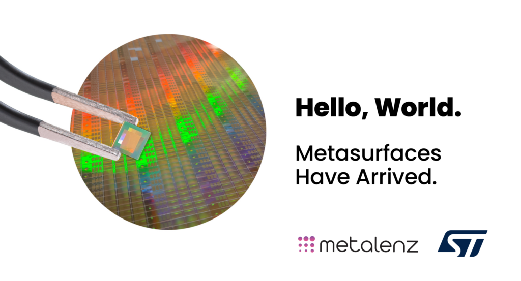
Potential applications of Metalenz metasurfaces extend beyond conventional optics, reaching into fields such as augmented reality and advanced sensor technology. The partnership with STMicroelectronics to develop the FlightSense module marks just one example of how this technology can be utilized in practical contexts that require precise measurements and data collection, paving the way for further advancements and capabilities in the tech sector.
Rob Devlin’s Vision and the Future of Optics
Rob Devlin’s journey from academic researcher to CEO of Metalenz illustrates the impact of visionary leadership in technology commercialization. His commitment to refining the mini-lens design has led to significant milestones, including the successful transition from lab prototypes to mass production. Devlin’s expertise in materials and nanofabrication has played a crucial role in optimizing the performance of metasurfaces, allowing Metalenz to remain competitive in a fast-evolving market.
Looking towards the future, Devlin’s focus on innovation continues to drive the roadmap for Metalenz. With new projects like Polar ID, which utilizes light polarization to enhance security features in smartphones, the potential for metasurfaces to revolutionize various industries is apparent. Devlin envisions an exciting era where technological advancements will enable new functionalities while democratizing high-quality optical features for the masses, going beyond niche markets into everyday consumer products.
Commercialization of Harvard Research
The commercialization of research conducted at Harvard, particularly in the field of optics, represents a unique synergy between academia and industry. The establishment of startups like Metalenz highlights the potential for groundbreaking discoveries to reach the market, fostering technological evolution directly rooted in scientific inquiry. This transition from theory to practical application is essential for the growth of new industries, as noted by Sam Liss from Harvard’s Office of Technology Development.
Moreover, the successful commercialization of devices like metasurfaces shows how university research can deliver tangible benefits, driving innovation that reaches consumers globally. The robust infrastructure built around Harvard’s research initiatives provides fertile ground for entrepreneurs like Devlin to transform concepts into viable technologies that enhance industries ranging from consumer electronics to health care and beyond.
The Role of Polarization Metasurfaces in Modern Technology
Polarization metasurfaces stand at the forefront of optical advancements, showcasing how new technologies can serve multifaceted purposes beyond traditional imaging. Rob Devlin’s exploration into this area highlights the potential for polarized light detection to secure personal devices, paving the way for innovative anti-counterfeiting measures in consumer electronics. Such capabilities are not just theoretical; they draw from solid scientific foundations established in research environments like the Capasso lab.
As the demand for advanced security features grows alongside the proliferation of smart devices, the implementation of cost-effective polarization metasurfaces could revolutionize how manufacturers design camera systems and security modules. This innovation ensures that even small devices can provide enhanced functionalities, making technology more accessible and effective without the hefty price tags typically associated with high-end optics.
How Metalenz is Changing the Lens-Making Industry
Metalenz’s emergence is pivotal in transforming the traditional lens-making industry, characterized by large curved glass or plastic components. The start-up’s successes demonstrate a clear trajectory toward replacing cumbersome lenses with more efficient, compact metasurfaces. This shift not only solves spatial constraints faced by manufacturers but also allows for the integration of advanced features in a more elegant package.
The competitive edge that Metalenz holds is attributable to its ability to streamline production and innovate continuously. As the company expands its partnerships and technological capabilities, it stands to disrupt the lens market significantly. The implications for various products—from smartphones to advanced imaging devices—are profound, heralding a new phase of design possibilities that align with growing consumer expectations for miniaturization and efficiency.
Consumer Electronics Innovation Fueled by Metalens Technology
The integration of metalens technology into consumer electronics symbolizes a significant leap in innovation, addressing consumer desires for enhanced functionality within smaller devices. By rethinking the standard optical components, Metalenz caters to manufacturers eager to elevate their product offerings while addressing the challenges of space constraints. This innovation enables a slew of applications, from improved camera capabilities to advanced sensor technologies that rely on precise light control.
As the landscape of consumer electronics continues to evolve rapidly, brands that adopt metalens technology are better poised to lead in a competitive market. The promise of reduced size and cost, alongside augmented performance, positions these devices at the forefront of the next generation of technology, blurring the lines between availability and cutting-edge innovation. This consumer electronics revolution stands to change how we interact with technology daily, propelling us into an era defined by sleek, efficient, and powerful devices.
The Future of Optical Disruption: Bringing Research to Market
The journey from academic research to market-ready products is a multifaceted one, characterized by collaboration and strategic vision. Metalenz exemplifies how research initiatives can fuel real-world innovation, focusing on disrupting traditional markets through unique and functional design. With its emphasis on leveraging established scientific principles around metasurfaces, Metalenz is not merely competing but redefining industries, showcasing the practical impact of academic research in everyday technology.
As we look forward, the importance of fostering environments that bridge the gap between theoretical research and practical application cannot be overstated. Devlin’s ongoing collaborations with academic institutions ensure a steady influx of insights and technological advancements that not only further optimize their current product offerings but pave the way for entirely new markets driven by cutting-edge research—reflecting a promising future for optics and consumer electronics alike.
Frequently Asked Questions
What are Metalenz metasurfaces and how do they differ from traditional lenses?
Metalenz metasurfaces are innovative optical devices that leverage mini-lens technology to focus light using a flat wafer embedded with tiny pillars, rather than traditional curved lenses made of glass or plastic. This groundbreaking design allows for a smaller, cheaper, and potentially mass-producible solution for consumer electronics, significantly disrupting the conventional lens-making industry.
How did Rob Devlin contribute to the development of Metalenz metasurfaces?
Rob Devlin, a graduate student at Harvard, played a crucial role in developing Metalenz metasurfaces while collaborating in Federico Capasso’s lab. He experimented with materials and prototypes to refine the mini-lens technology, ultimately co-founding Metalenz in 2016, where he now serves as CEO, facilitating the commercialization of this innovative technology for consumer electronics.
What are some applications of Metalenz metasurfaces in consumer electronics?
Metalenz metasurfaces are used in various consumer electronics, such as smartphones, tablets, and other devices. They enhance features like 3D sensing modules in devices like the iPad and Samsung Galaxy S23 Ultra, enabling facial recognition, augmented reality, and improved depth perception for camera systems.
How has Harvard’s research contributed to the commercialization of Metalenz metasurfaces?
Harvard’s cutting-edge research, particularly in the Capasso lab, laid the foundational work for Metalenz metasurfaces. The collaboration between researchers like Rob Devlin and Federico Capasso led to the successful transition from a research prototype to mass manufacturing, bringing innovative mini-lens technology to real-world consumer products.
What is Polar ID and how does it relate to Metalenz metasurfaces?
Polar ID is an upcoming application of Metalenz’s polarization metasurfaces designed to enhance smartphone security. By leveraging light polarization, this technology offers a compact and affordable solution for unique identification, allowing devices to detect distinct polarization signatures that distinguish individuals, thus improving security features.
What challenges does Metalenz face in the competitive optics industry?
As a leader in metasurfaces, Metalenz faces competition from other companies attempting to catch up with their technology. To maintain their edge, Metalenz focuses on continuous improvement of existing products, developing innovative new applications for metasurfaces, and benefiting from ongoing research collaborations with the Capasso lab.
Are Metalenz metasurfaces cost-effective compared to traditional lenses?
Yes, Metalenz metasurfaces are designed to be significantly more cost-effective than traditional lenses. For instance, while conventional polarization cameras can cost between $500 and $1,000, Metalenz’s polarization metasurface measures just 5 millimeters and costs around $5, making it accessible for widespread adoption in numerous consumer devices.
What potential does Metalenz’s technology have for future products?
The potential of Metalenz’s metasurfaces lies in their ability to condense complex optical modules into compact formats while unlocking entirely new functionalities. As the technology evolves, there are exciting prospects for diverse applications, from improved health monitoring tools to enhanced consumer electronics.
How does Metalenz plan to innovate and expand its product line?
Metalenz plans to innovate and expand its product line by continuously enhancing current products, exploring new applications for metasurfaces, and leveraging ongoing research from their founding lab at Harvard. Their strategy involves staying ahead in a competitive market while maximizing the unique properties of their technology.
What impact have Metalenz metasurfaces had on the optics industry?
Metalenz metasurfaces have had a significant impact on the optics industry by providing a new paradigm for light manipulation. Their ability to create smaller, lighter, and more efficient optical systems is changing how manufacturers design consumer electronics, allowing for more advanced features without the constraints of bulky traditional lenses.
| Key Point | Details |
|---|---|
| Introduction to Metalenz | Founded in 2016, focuses on innovative mini-lenses (metasurfaces) developed from research at Harvard University. |
| Development of Metalenses | Rob Devlin created 100 prototypes, which were designed to be smaller and more cost-effective than traditional lenses. |
| Commercial Success | Produced around 100 million metasurfaces, utilized in devices like iPad, Samsung Galaxy S23 Ultra, and Google Pixel 8 Pro. |
| Innovation Impact | Metalenz aims to disrupt the lens-making market by replacing bulky glass and plastic lenses with efficient metasurfaces. |
| Strategic Partnerships | Collaborated with STMicroelectronics to create a distance-measuring module that uses light sensing for applications like facial recognition. |
| Future Developments | Working on Polar ID technology to enhance smartphone security while reducing size and cost. |
| Challenges and Competition | Facing competition from other tech companies but leveraging existing products and continued innovation. |
Summary
Metalenz metasurfaces represent a transformative leap in optical technology, evolving from cutting-edge research to widely adopted solutions in consumer electronics. Founded on innovative designs that challenge traditional lenses, Metalenz plays a pivotal role in enhancing device functionalities while reducing costs and sizes. As the demand for compact sensor technologies grows, the future of Metalenz seems promising with ongoing advancements in applications like Polar ID which aim to redefine security in smartphones and other devices. This trajectory not only highlights the potential impacts of university research on industries but also exemplifies the shift toward more efficient and capable optical systems.